 |
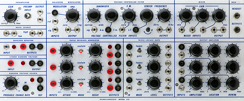
Buchla 212 Dodeca Module |
|
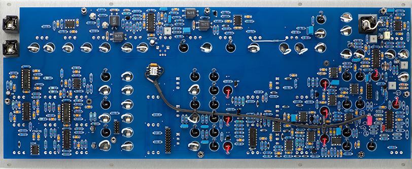
I repaired a 212 Dodeca module and I also built a Dodeca module. The customer sent me a complete kit of parts and I assembled and tested the module. Many of the components are sourced through Mouser but specialized parts, panel, knobs, and PCBs have specific sourcing and I do not know the details.
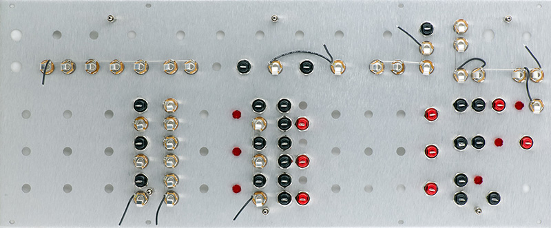
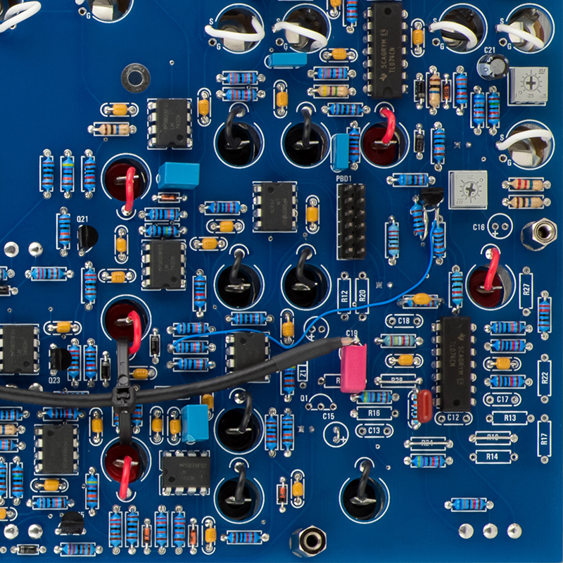
This panel has a lot of components so to simplify assembly I bussed the 3.5mm grounds in logical groups.
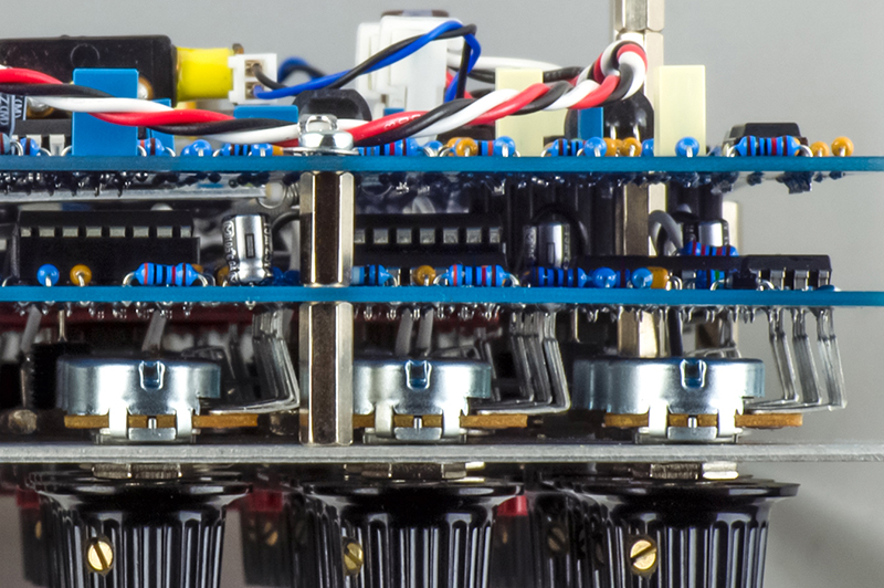
I used 15mm spacers from the panel to PCB1. I see some information where people are using 17mm but I chose 15mm. With 15mm there is a bit of thread above the nuts for the switches.
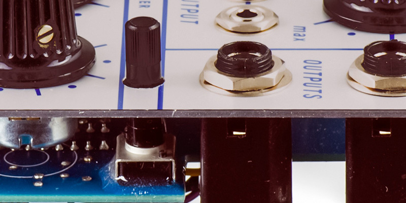
The potentiometer leads don't line up and you don't want to stress the potentiometers because the phenolic will fracture. I rebent the leads to 90° on othe modules but chose to bend them in a semi-Z pattern. With a spacer nut on the potentiometer, there is limited clearance when using 15mm spacers so I left them off. The leads solder flush with the PCB as can be seen in this side image (what looks like a lead extending through the PCB is actually the resistor lead behind the potentiometer). This leaves ample room for the washer and nut on the panel.
Mounting the panel was a real bear. As usual, I first installed the switches, lined them up, and then soldered them. I then installed all the potentiometers and only soldered the middle lead. I installed the LEDs and bent the leads together but did not solder them. Then I lined up all the wires from the 3.5mm jacks and pulled them through their respective holes. I started at one end of the PCB and lined up the potentiometers using a long rod or a long hook. Work slowly across the PCB aligning more shafts with enough pressure to keep the shafts in the holes. After you get all the shafts and switches aligned, make a second pass to align the bushings in the hole. When the PCB gets close enough to the panel you can put the standoffs on by a couple of threads to keep the PCB in place. Eventually you will get the panel all the way down. Check the LEDs to make sure they are aligned and not bent. Put the washer and nut on the potentiometers and reflow the center pin to relieve any stress. Then solder the outer two pins. It took about an hour to get it all together.
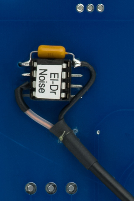
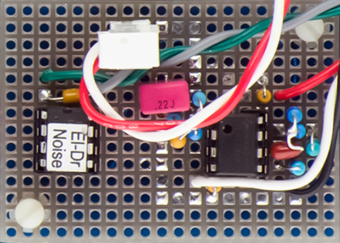
This image shows the rear of PCB1 with the Electric Druid noise modification as described below. You can also see the addition of the 11K5 resistor for the Balanced Modulator control.
PCB is pretty straightforward to build. The LM307 and CA3080 are can style packages. I used MTA connectors for the headphone and outputs.
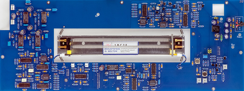
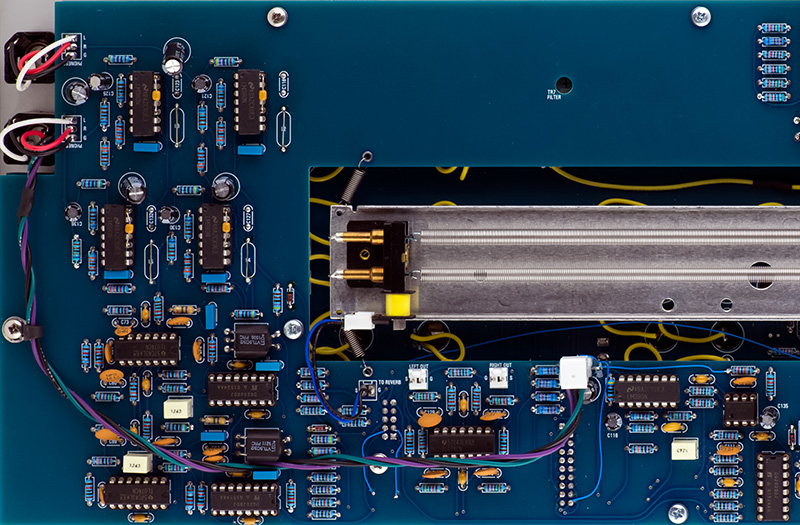
The revert tank is a Beltron/Accutronics 1BC2E which is 150R input impedance, 10K output impedance, and 1.75 - 3 seconds per the datasheet.
Beltron/Accutronics 1BC2E datsheet
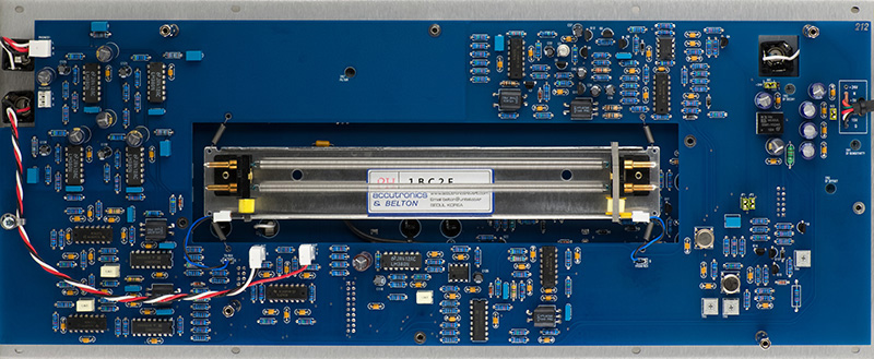
Here is the rear of the finished module.
Critical Modifications
Optional Modifications The noise circuit has very high gain and picks up a lot of crosstalk from the LEDs so the noise suffers from loud clicks. I could not find a simple means to eliminate this interference so modified the built module by adding a separate noise circuit using the Electric Druid noise chip (the issue with modifying a built module is it is difficult to remove the radial capacitors). I modified the unbuilt module with a number of modifications on PCB1 to implement the same circuit. I changed the suggested schematic on the Electric Druid datasheet slightly to improve performance. To modify an unbuilt board:
|
The noise circuit I used is a modification of that on the Electric Druid datasheet. I had issues with DC restoration and hum on the outputs so I changed the first op-amp to an inverting configuration to improve performance.
Electric Druid noise circuit schematic
For the unassembled module I epoxied an 8 pin socket to a bare area near the +5V. I drilled holes in the board to run the wires for +5V and N directly to the connector pins on the opposite side. I used shielded cable for the noise signal and tied it to the PCB to not strain the socket leads.
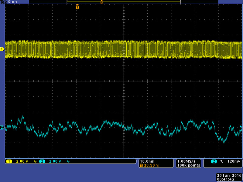
This portion of PCB1 shows the noise and envelope detector modifications as described above. The white output is 2V pk-pk and the pink output is just a bit hotter so they sound similar in level.
For the assembled module I added a small hand-built noise circuit using the Electric Druid IC and wired it to the front panel jacks by removing R10 and R11 on PCB1.
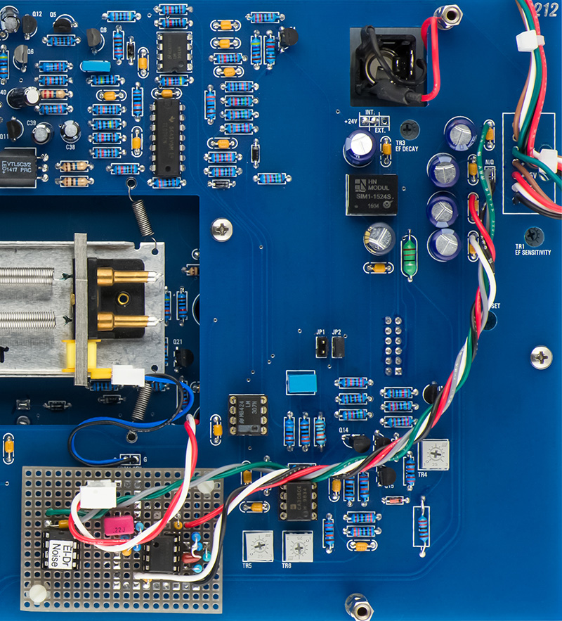
I added the noise PCB to the bottom of PCB2 and ran wires to PCB1 using an MTA connector so you can still separate the PCBs for service. I also had to modify R15 on PCB1 so the noise for the Random Voltage Source would use the new white noise signal. I ran the power wires directly to the decoupling capacitors to minimize any crosstalk from the other circuits.
Operation and Calibration
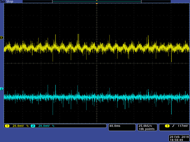
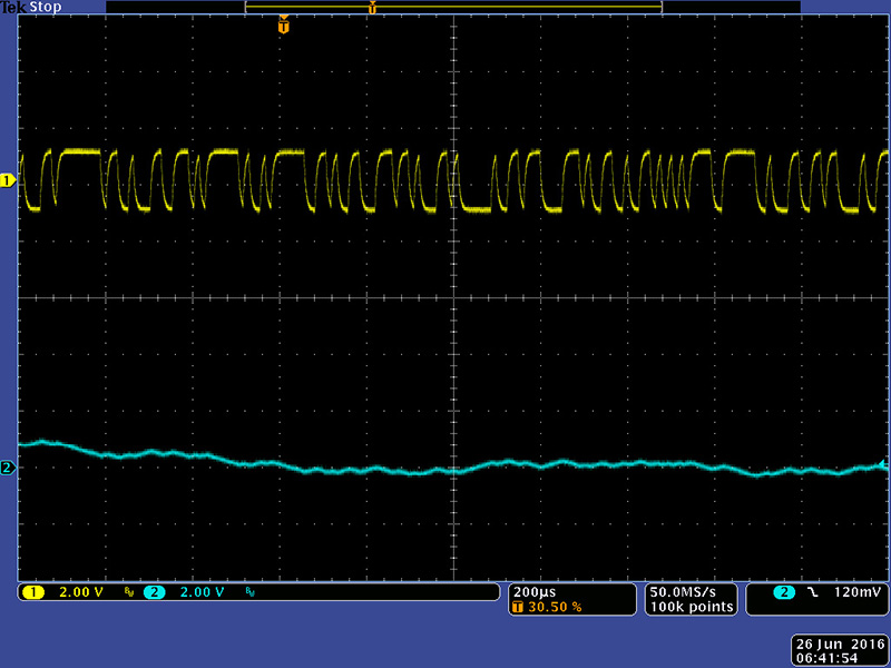
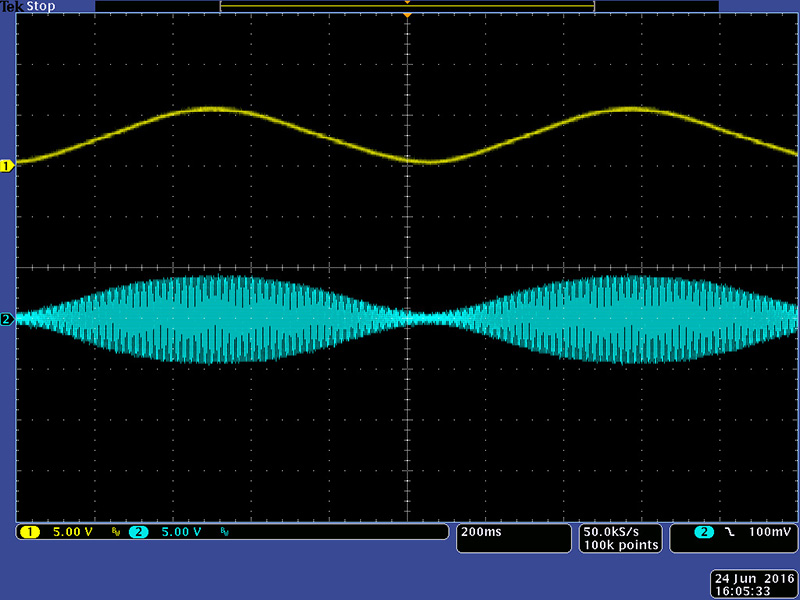
The noise circuit works quite well. This scope image shows the High (white) and Low (pink) outputs.
Here is a more detailed image of High (white).
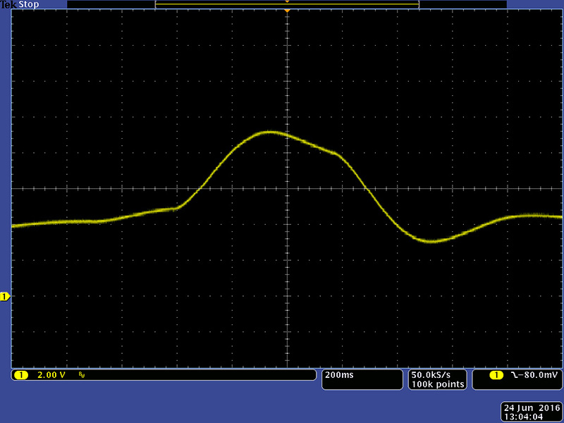
The Envelope Detector has three calibration adjustments. TR2 EF Offset is adjusted for 0V on the output with no input. TR1 Sensitivity is adjusted to preference for signal level. TR3 EF Decay is also adjusted to preference for decay. I have decay adjusted very low so the envelope follows the amplitude quite closely as seen in this scope image.
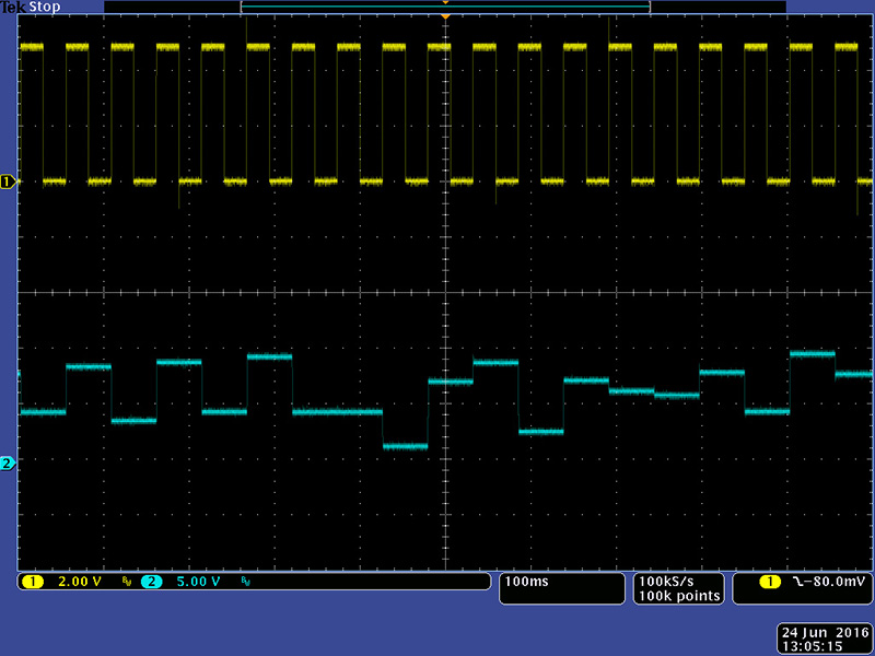
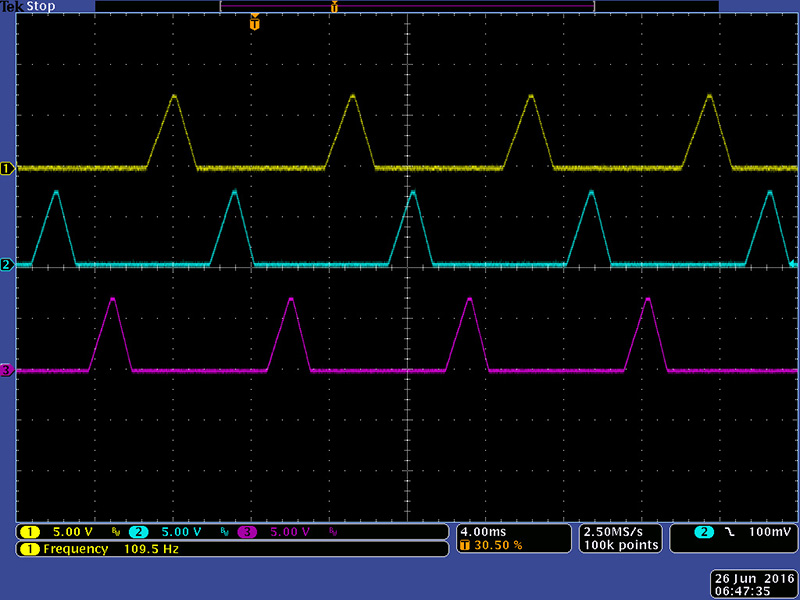
The Stored Random Voltage output changes on every rising edge clock as can be seen in this scope image.
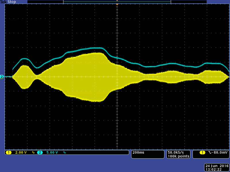
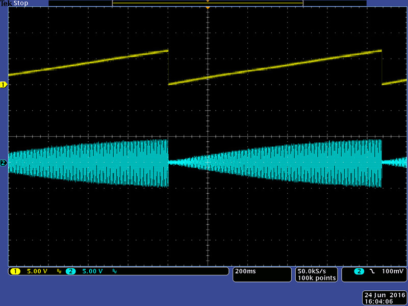
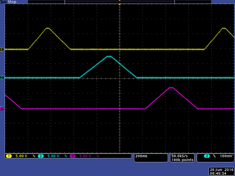
The Random Voltage Source is derived from the Low Noise. The Probable Rate Of Change determines the frequency and smoothness of the changes. This scope image shows the output with the control full clockwise.
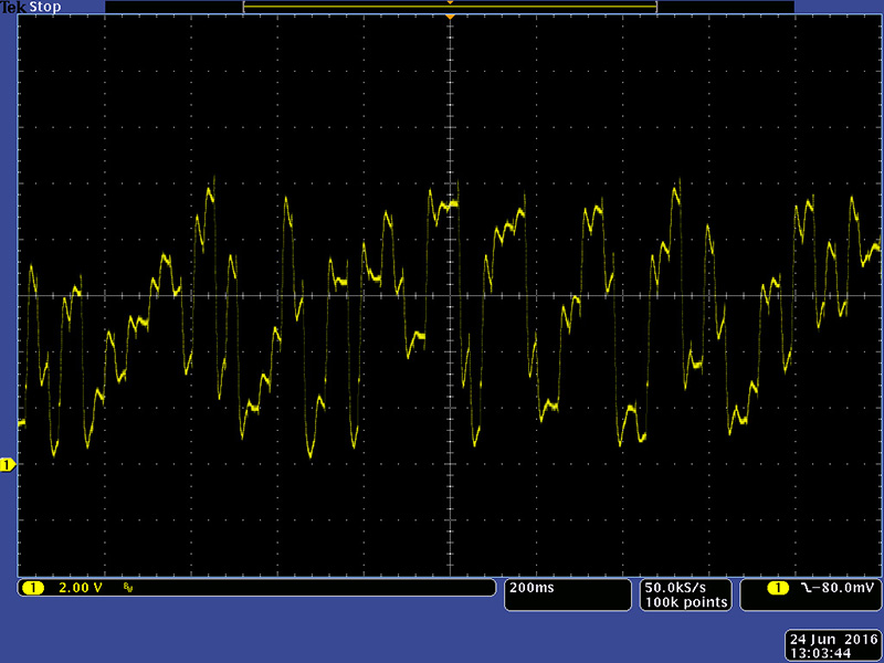
This image shows a much smoother and less frequent change when the control is at mid position.
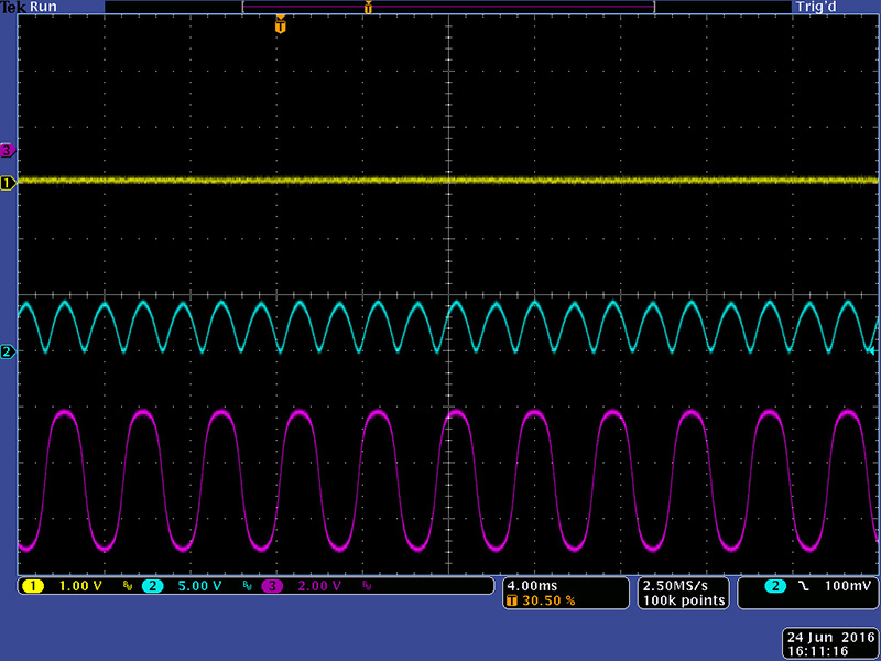
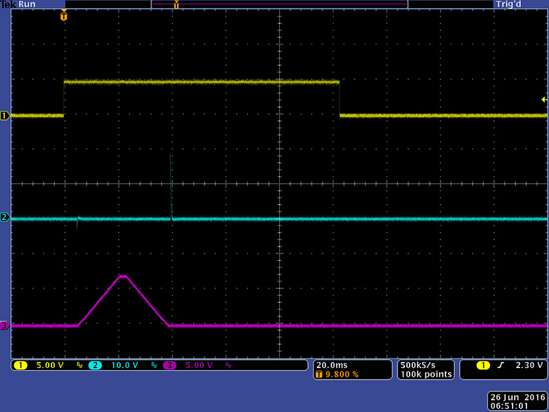
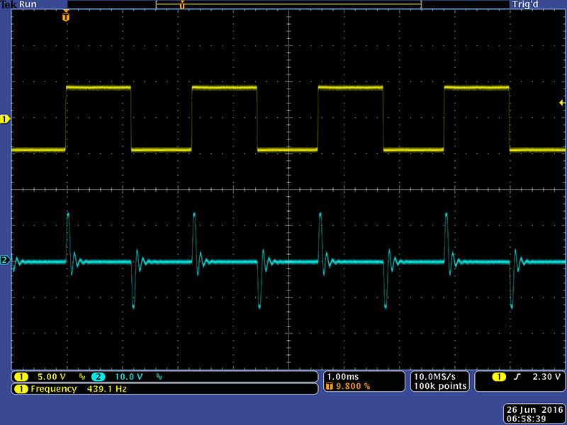
Calibration of the Balanced Modulator seems to be complex. I have calibrated two modules where I could not follow the published procedure at all. The circuit consists of a current source controlled by TR4, and differential pair with an input controlled by TR5, an OTA with an offset controlled by TR6, and a recovery differential op-amp for the current to voltage conversion from the OTA (- input) and the Signal. (+ input). With a signal input, the output is 0V when the OTA level matches the Signal input level to the OTA. For OTA output voltage < Signal input voltage, the resulting signal output is negative (inverted). For OTA output voltage > Signal input voltage, the resulting signal output is positive (non-inverted). Thus the OTA has to be biased to an on state for the output to be 0V. I ended up calibrating the Balanced Modulator using this method:
Remove JP1 and JP2. Measure the output voltage with no inputs and adjust TR6 for 0.0V output.
Adjust the Amp control to full CW (RM position) with no inputs. Measure the differential voltage between the base of Q14 and Q15 and adjust TR5 until the voltage is 0.0V. Note I had to decrease R117 from 220K to 68K to be able to make this adjustment. The base of Q14 can be probed on the left end of R120 and the base of Q15 can be probed on the top end of R119.
Install JP2. Plug a sine wave source into both the Signal and Ref input and leave the Amp control on RM. Monitor the output with an oscilloscope and adjust TR4 until a positive sine wave of 2X frequency occurs. TR4 will adjust the alternate peaks so adjust for equal height as can be seen in this oscilloscope image. The bottom magenta trace is the voltage on the collector of Q14 and represents the Iabc current for the OTA.
Leave JP2 installed and JP1 removed for normal operation.
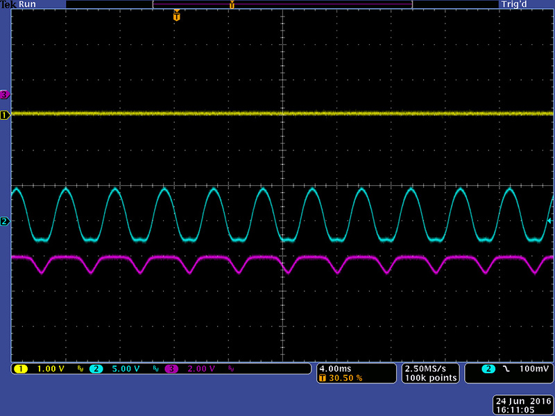
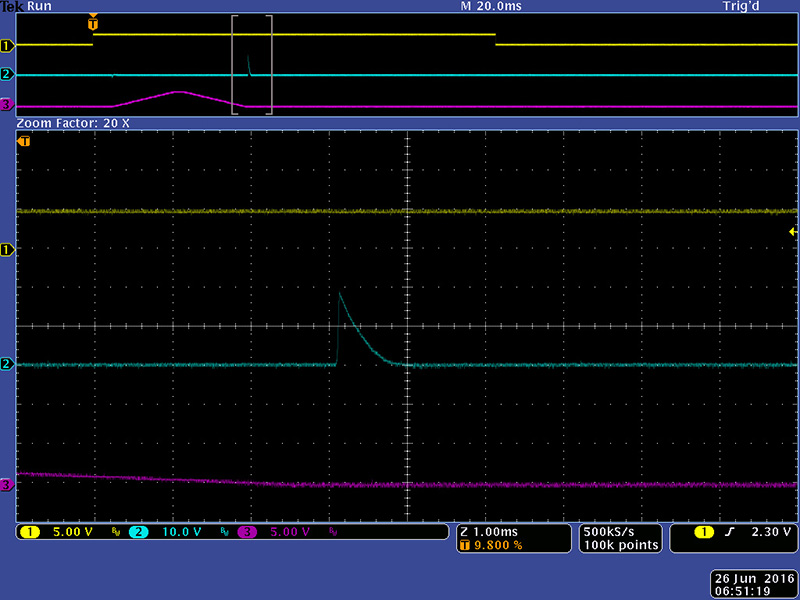
When you adjust the Amp control to Zero the output should just be the Signal input. It has a bit of lower voltage distortion as can be seen in this scope image. The voltage on the collector of Q14 has a bit of the Signal input as some bleeds to the CV input. You can adjust TR4 to minimize but then your peaks in Ring Mode will not be of equal height. Note you can adjust TR4 such that the Amp control reverses so increasing VCA gain occurs for decreasing CV and CCW rotation.
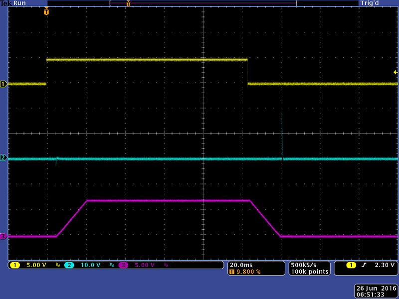
This scope image shows the Balanced Modulator as a VCA The control voltage cannot quite shut the VCA off completely.
This scope image shows the VCA with a sine control voltage.
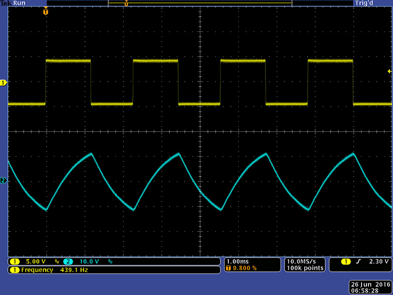
The Triple Envelope Generators require no calibration. This scope image shows the non-sustain mode where decay follows attack. The outputs are only 7V. You can increase them to 10V by changing R172, R197, and R222 from 10K to 3K3.
Here is a detailed look at the Trigger Output pulse.
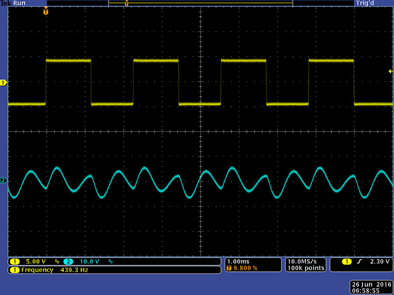
Here is a scope image of sustain where the decay does not start until the input gate goes false.
You can plug the Trigger Output (red) into the Trigger Input (red) for a free-running oscillator. The Sustain switch may need to be momentarily set to down to start the cycle. Here I have sequenced all three EGs.
The maximum frequency when sequencing all three is about 110 Hz.
The VCF has one calibration which trims the fixed resonance. I have it set to maximum. This scope image shows the VCF output with Bandwidth set to about 30% rotation and the Center Frequency set to low.
This scope image shows the VCF output with Bandwidth set to about 30% rotation and the Center Frequency set to mid. You can see the effect of the resonance well at this setting.
This scope image shows the VCF output with Bandwidth set to about 30% rotation and the Center Frequency set to high.
Reverb Return Modification
The reverb return is always at maximum which adds noise to the output. A customer wanted me to add a reverb return. There is space just below the headphone jacks so I mounted a Bourns 20K linear black plastic shaft potentiometer (Mouser PN 652-PTV09A-4030UB203) similar to the Q control. I reversed the bend on the leads so they pointed up and cut them off short. I trimmed the metal soldering brackets flush with the back and flattened the three plastic nibs on the rear so it was flush. I drilled a hole in line with the Headphone jacks and between the two blue lines. You can lift the panel enough to slide the potentiometer with wires attached into position. I oriented the leads towards the center of the module (this rotates the index line on the top of the potentiometer to about the 11 o'clock position when off) and used epoxy to glue the potentiometer to PCB1. When dry I added a bit more epoxy on the three sides. I routed the wires up through the Output jack hole in PCB1.
The Reverb Return control looks quite natural on the panel. It is just a bit shorter than the Q control since it is mounted flush to the PCB.
This front close-up and profile shows the Reverb Return shaft.
This photo shows the potentiometer glued to the PCB on three sides.
Cut the run on the rear of PCB2 between R403 and R411. Connect the CW terminal of the reverb return potentiometer to the left side of R403. Connect the wiper of the reverb return potentiometer to the right side of R411. Connect the CCW terminal of the reverb return potentiometer to ground. Ground is located on pin 20 (lower right) of PLD2. I brought the reverb return wires through the headphone jack notch and epoxied a 3 pin MTA to PCB2 so I could easily disconnect the PCBs (ignore the extra wires and modes as this is the first 212 prototype).
The noise floor is quite low with the reverb return potentiometer off.